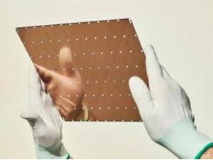
New artificial intelligence company Cerebras Systems is unveiling the largest semiconductor chip ever built.
The Cerebras Wafer Scale Engine has 1.2 trillion transistors, the basic on-off electronic switches that are the building blocks of silicon chips. Intel’s first 4004 processor in 1971 had 2,300 transistors, and a recent Advanced Micro Devices processor has 32 billion transistors.
Most chips are actually a collection of chips created on top of a 12-inch silicon wafer and are processed in a chip factory in a batch. But the Cerebras Systems chip is a single chip interconnected on a single wafer. The interconnections are designed to keep it all functioning at high speeds so the trillion transistors all work together as one.
In this way, the Cerebras Wafer Scale Engine is the largest processor ever built, and it has been specifically designed to process artificial intelligence applications. The company is talking about the design this week at the Hot Chips conference at Stanford University in Palo Alto, California.
Samsung has actually built a flash memory chip, the eUFS, with 2 trillion transistors. But the Cerebras chip is built for processing, and it boasts 400,000 cores on 42,225 square millimeters. It is 56.7 times larger than the largest Nvidia graphics processing unit, which measures 815 square millimeters and 21.1 billion transistors.
The WSE also contains 3,000 times more high-speed, on-chip memory and has 10,000 times more memory bandwidth.
The chip comes from a team headed by Andrew Feldman, who previously founded the micro-server company SeaMicro, which he sold to Advanced Micro Devices for $334 million. Sean Lie, cofounder and chief hardware architect at Cerebras Systems, will provide an overview of the Cerebras Wafer Scale Engine at Hot Chips. The Los Altos, California company has 194 employees.
Chip size is profoundly important in AI, as big chips process information more quickly, producing answers in less time. Reducing the time to insight, or “training time,” allows researchers to test more ideas, use more data, and solve new problems. Google, Facebook, OpenAI, Tencent, Baidu, and many others argue that the fundamental limitation of today’s AI is that it takes too long to train models. Reducing training time thus removes a major bottleneck to industrywide progress.
Of course, there’s a reason chip makers don’t typically build such large chips. On a single wafer, a few impurities typically occur during the manufacturing process. If one impurity can cause a failure in a chip, then a few impurities on a wafer would knock out a few chips. The actual manufacturing yield is just a percentage of the chips that actually work. If you have only one chip on a wafer, the chance it will have impurities is 100%, and the impurities would disable the chip. But Cerebras has designed its chip to be redundant, so one impurity won’t disable the whole chip.
“Designed from the ground up for AI work, the Cerebras WSE contains fundamental innovations that advance the state-of-the-art by solving decades-old technical challenges that limited chip size — such as cross-reticle connectivity, yield, power delivery, and packaging,” said Feldman, who cofounded Cerebras Systems and serves as CEO, in a statement. “Every architectural decision was made to optimize performance for AI work. The result is that the Cerebras WSE delivers, depending on workload, hundreds or thousands of times the performance of existing solutions at a tiny fraction of the power draw and space.”
These performance gains are accomplished by accelerating all the elements of neural network training. A neural network is a multistage computational feedback loop. The faster inputs move through the loop, the faster the loop learns, or “trains.” The way to move inputs through the loop faster is to accelerate the calculation and communication within the loop.
“Cerebras has made a tremendous leap forward with its wafer-scale technology, implementing far more processing performance on a single piece of silicon than anyone thought possible,” said Linley Gwennap, principal analyst at the Linley Group, in a statement. “To accomplish this feat, the company has solved a set of vicious engineering challenges that have stymied the industry for decades, including implementing high-speed die-to-die communication, working around manufacturing defects, packaging such a large chip, and providing high-density power and cooling. By bringing together top engineers in a variety of disciplines, Cerebras created new technologies and delivered a product in just a few years, an impressive achievement.”
With 56.7 times more silicon area than the largest graphics processing unit, Cerebras WSE provides more cores to do calculations and more memory closer to the cores so the cores can operate efficiently. Because this vast array of cores and memory is on a single chip, all communication is kept on-silicon, which means its low-latency communication bandwidth is immense, so groups of cores can collaborate with maximum efficiency.
The 46,225 square millimeters of silicon in the Cerebras WSE house 400,000 AI-optimized, no-cache, no-overhead, compute cores and 18 gigabytes of local, distributed, superfast SRAM memory as the one and only level of the memory hierarchy. Memory bandwidth is 9 petabytes per second. The cores are linked together with a fine-grained, all-hardware, on-chip mesh-connected communication network that delivers an aggregate bandwidth of 100 petabits per second. More cores, more local memory, and a low-latency high-bandwidth fabric together create the optimal architecture for accelerating AI work.
The Cerebras WSE’s record-breaking achievements would not have been possible without years of close collaboration with TSMC, the world’s largest semiconductor foundry, or contract manufacturer, and leader in advanced process technologies, the companies said. The WSE is manufactured by TSMC on its advanced 16nm process technology.


